Quantum NIL Unleashes the Potential of NIL Nanoimprint Technology
Innovative technology - 2025-09-10
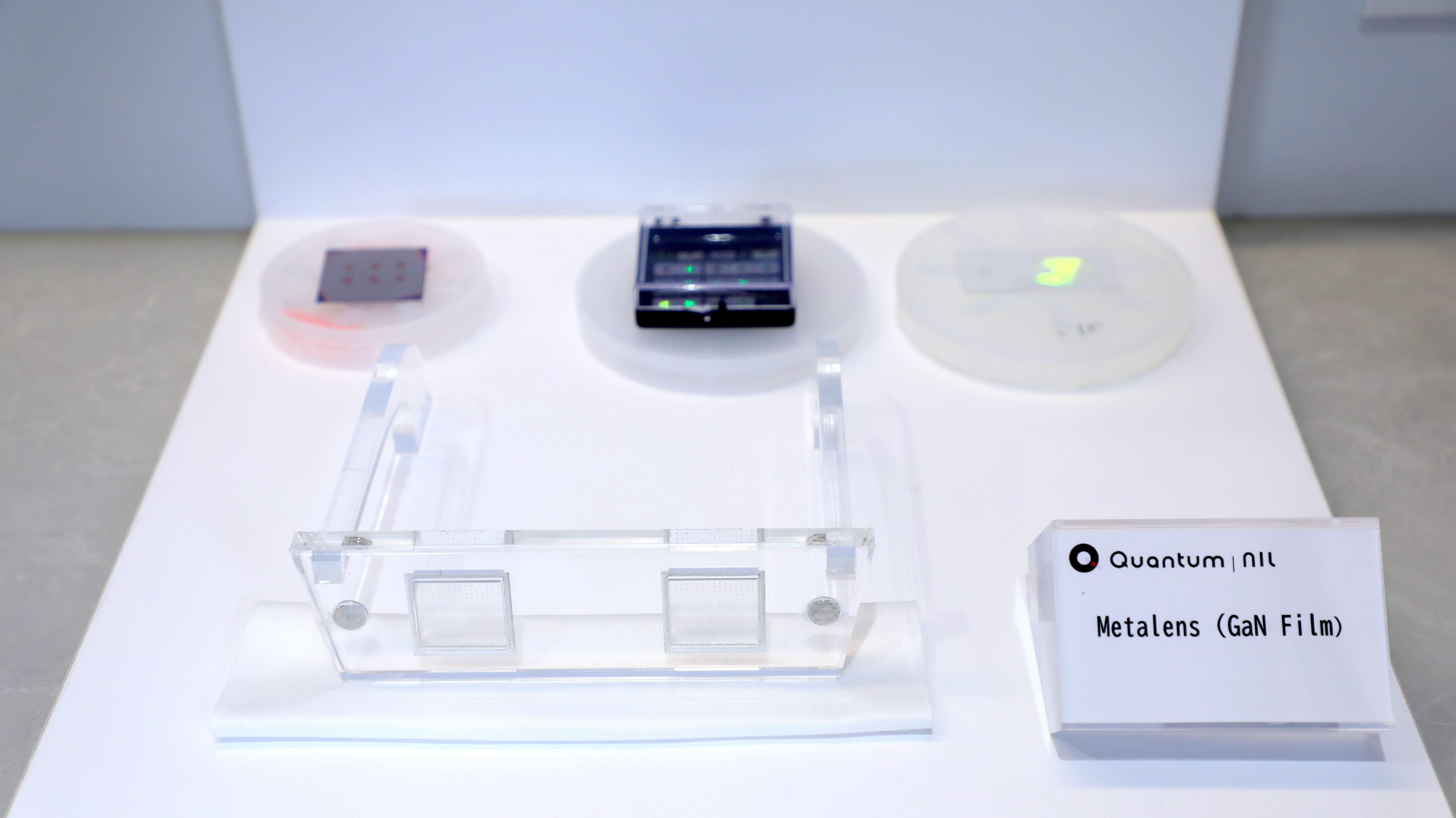
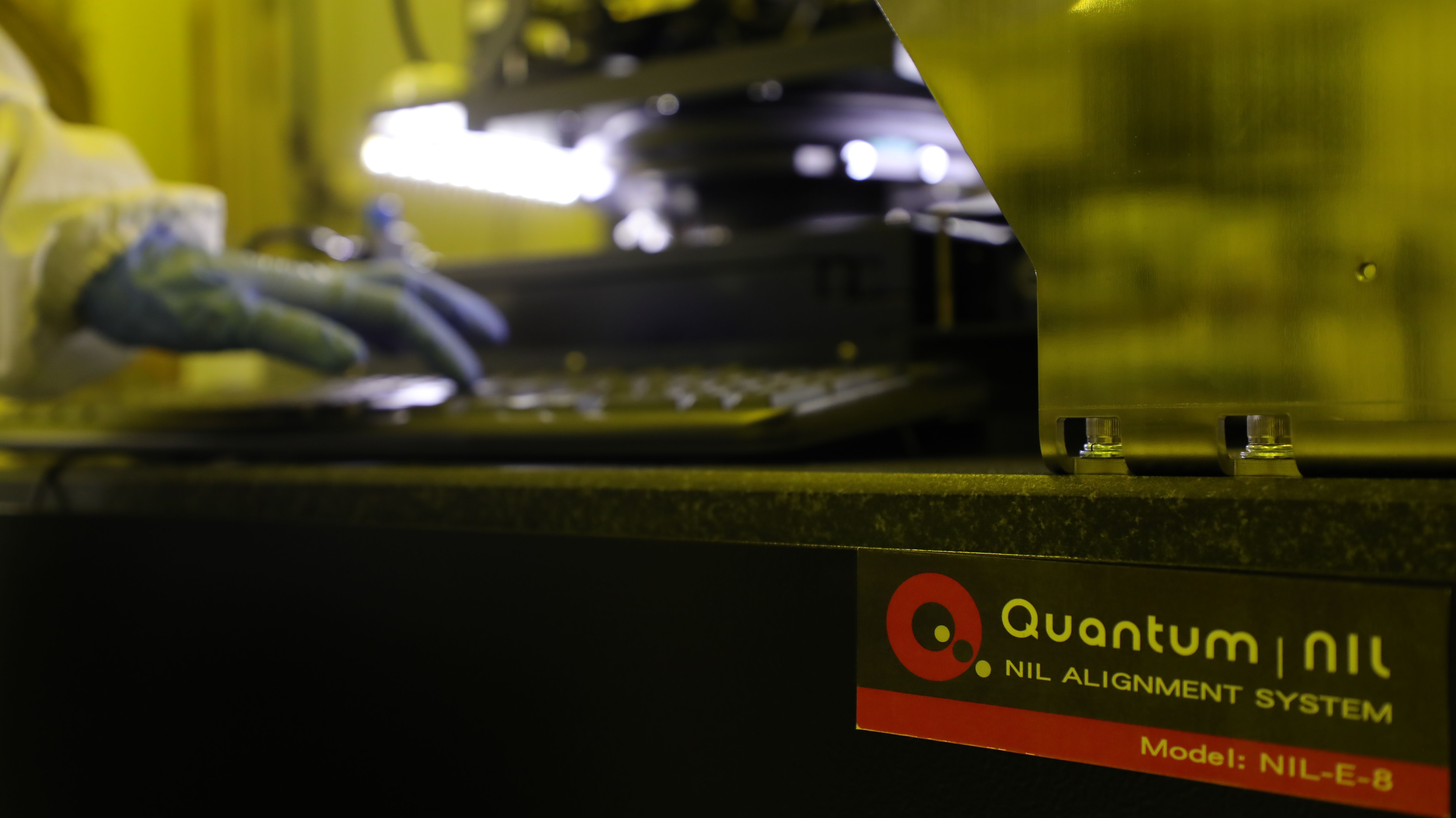
Quantum NIL specializes in nanoimprint technology, providing professional contract manufacturing services for high-end nanopatterns for high-tech products such as AI chips, AR glasses, and metalens (Image: Provided by Quantum NIL)
Future AI-driven chips, AR glasses, and even quantum optical devices are likely to be manufactured using "imprinting" methods. As AI and quantum technologies advance rapidly, traditional mass-production methods are struggling to keep pace with the versatile demands of AI design. Nanoimprint Lithography (NIL), a groundbreaking manufacturing process, is becoming the key to building next-generation electronic and optical devices. By creating ultra-fine and high-precision structures with low cost and a low carbon footprint, NIL enhances performance while offering superior energy efficiency and flexibility.
Quantum NIL has deeply specialized in the field of nanoimprint technology, providing high-end nanopatterning foundry services for high-tech products such as AI chips, AR glasses, and Metalenses. With a team boasting extensive experience in materials science and compound semiconductors, the company can produce complex and precise nano-structures tailored to specific client needs. As global demand for power-saving, high-performance optoelectronic products rises, Quantum NIL is leveraging its vision and technical prowess to bolster Taiwan's international standing and competitiveness in nano-manufacturing.
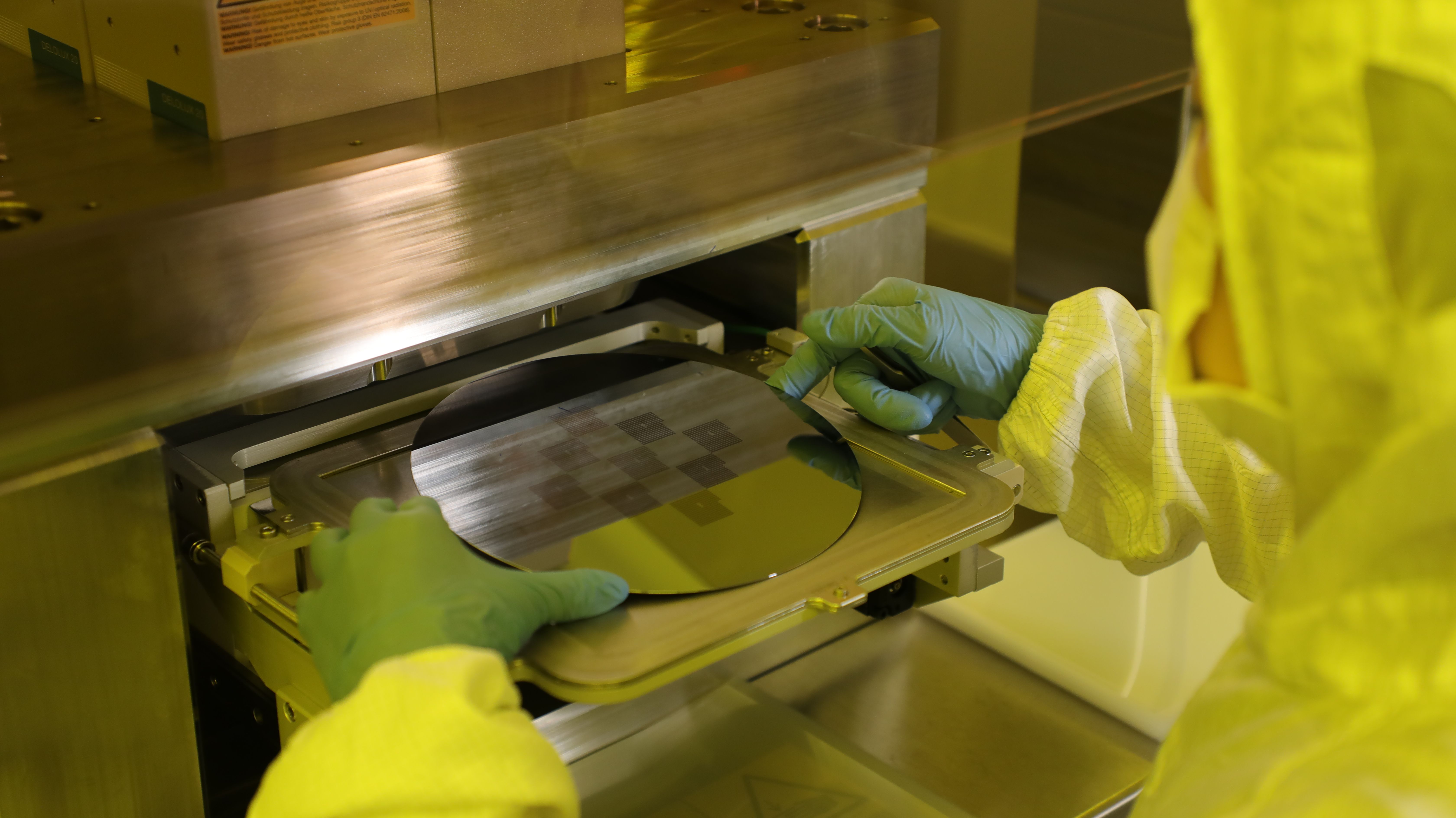
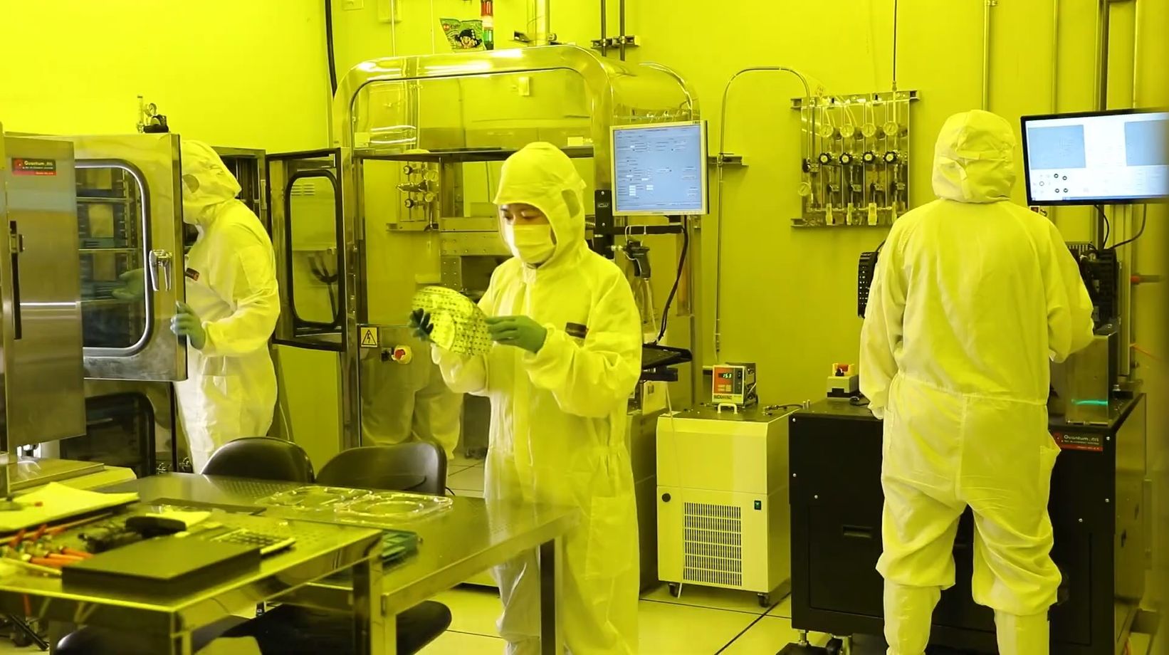
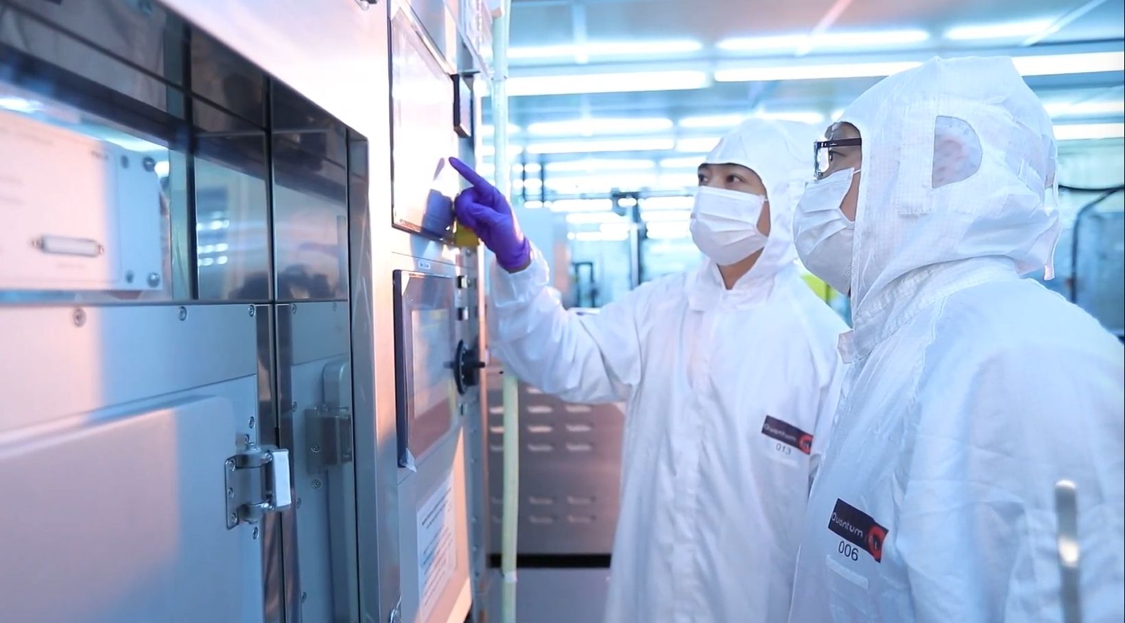
Quantum NIL continues to innovate by expanding the applications of nanoimprint technology, building core competitiveness through its "Hybrid Nanoimprint" solutions. Photo provided by Quantum NIL.
One of the founders, Dr. Sean Lin, holds a B.S. in Physics from National Taiwan University and a Ph.D. in Physics from New York University. An expert in photonic crystal theory and manufacturing, Dr. Lin previously served as General Manager of the Nanoimprint Business Group at IQE in the UK and at Arima Optoelectronics in Taiwan. He has channeled over 20 years of expertise in the optoelectronic semiconductor field into the foundation of Quantum NIL.
Dr. Lin points out that as AI-driven design methods evolve rapidly, they are leading quantum technology toward highly complex and quasi-random design architectures that optimize system integration and performance.
This trend in AI design presents new challenges for traditional photolithography, which struggles to meet the requirements of highly diverse structural designs and ultra-small patterns. Traditional lithography not only faces barriers in resolving complex patterns but also finds it difficult to balance flexibility, efficiency, and cost control, making it hard to scale for low-volume, high-variety production needs.
Quantum NIL’s Hybrid Nanoimprint technology offers exceptional flexibility and cross-material compatibility. It can be integrated with biopolymers, thermal/photoresists, metals, plastics, glass, compound semiconductors, metal oxides, composite materials, and bio-functional materials. Furthermore, the process is applicable to wafers with geometric warping or significant thickness variations, as well as non-flat and curved substrates—surpassing the process adaptability of traditional photolithography.
NIL transfers patterns mechanically by pressing a patterned template or mold into a polymer or resist layer. Since it does not rely on optical imaging, it is particularly suited for manufacturing sub-wavelength nano-structures and avoids the need for complex Optical Proximity Correction (OPC), thereby simplifying the overall process. Dr. Sean Lin stated that compared to traditional photolithography, NIL does not require expensive equipment or cumbersome procedures, making it an ideal choice for startup R&D. Furthermore, compared to DUV and EUV processes, NIL consumes significantly less energy and gas while achieving similar critical dimensions (CD).
As early as 2006, Nanoimprint Lithography (NIL) demonstrated its immense potential by creating 2nm ultra-fine structures and microscopic components. As a pioneer in NIL technology, Quantum NIL continuously strengthens its process solutions and integrates nanoimprinting with traditional manufacturing methods. Their "Hybrid Nanoimprint" solution bridges the gap between these technologies. Through continuous innovation, Quantum NIL is expanding the reach of nanoimprint technology and building a formidable competitive platform for nano-manufacturing.