Products & Services
NANO-FABRICATION FOUNDRY SERVICE
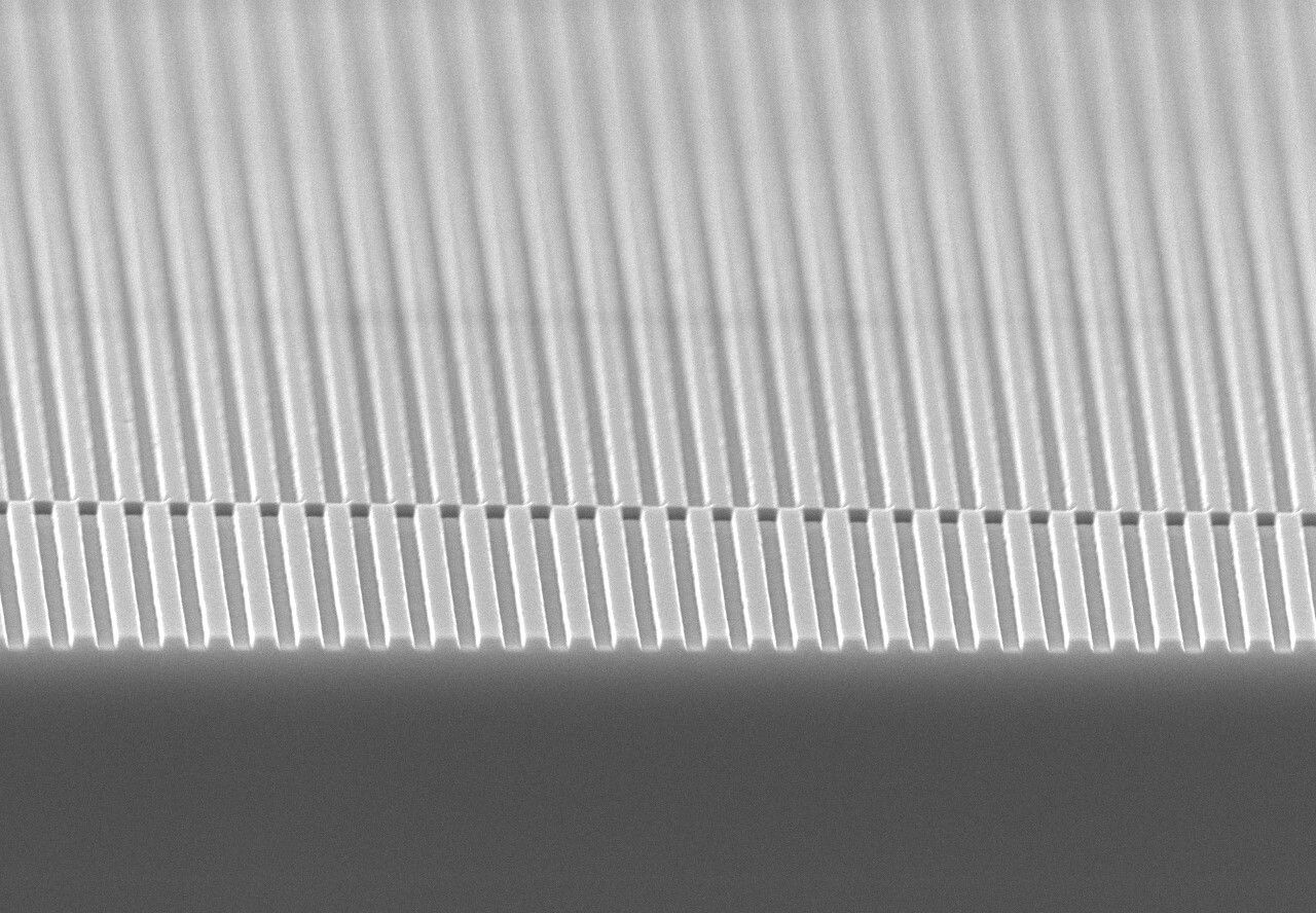
Grating Fabrication for DFB/VCSEL Epitaxy Wafer
- NIL & Photo-litho Process
- III-V Material Etch
- Process & Alignment Mark Fabrication
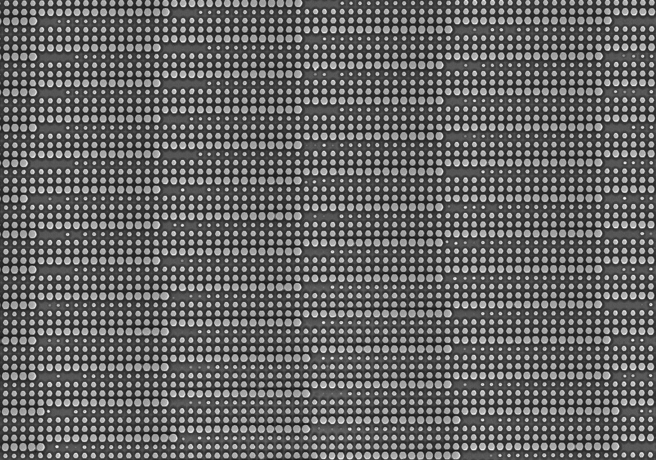
Diffractive Optical Element (DOE) & Metalens
- Optical Design Simulation
- NIL Process
- Glass/Quartz Material Etch
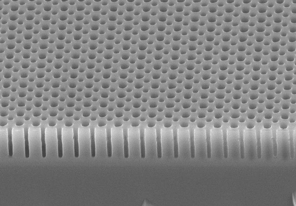
Photonic Crystal Fabrication
- Photonic Crystal & Photonic Quasi-crystal Design Simulation
- NIL & Photo-litho Process
- III-V Material Etch
Customized Nano-Textured Hybrid Fabrication
- Display & Light engine
- μLED & QD LED
- Bio-sensing/Detection Template
- Biomimetic Surface
SERVICE TECHNIQUES & SPECIFICATIONS
Production Scale of NIL
(2" ~ 8" wafer size)

(2" ~ 8" wafer size)
E-beam Lithography
& Photo Lithography
& Photo Lithography
Material Etch
Nano-structure Design
& Simulation
& Simulation